- 您现在的位置:买卖IC网 > Sheet目录1991 > CS5528-ASZR (Cirrus Logic Inc)IC ADC 24BIT 8CH 24-SSOP
CS5521/22/23/24/28
DS317F8
43
1.8 Power Supply Arrangements
The CS5521/22/23/24/28 A/D converters are de-
signed to operate from a single +5 V analog supply
and a single +5 V or +3 V digital supply. A -2.1 V
supply is usually generated from the charge pump
drive to provide power to the instrumentation am-
plifier’s
NBV
(negative
bias
voltage)
pin.
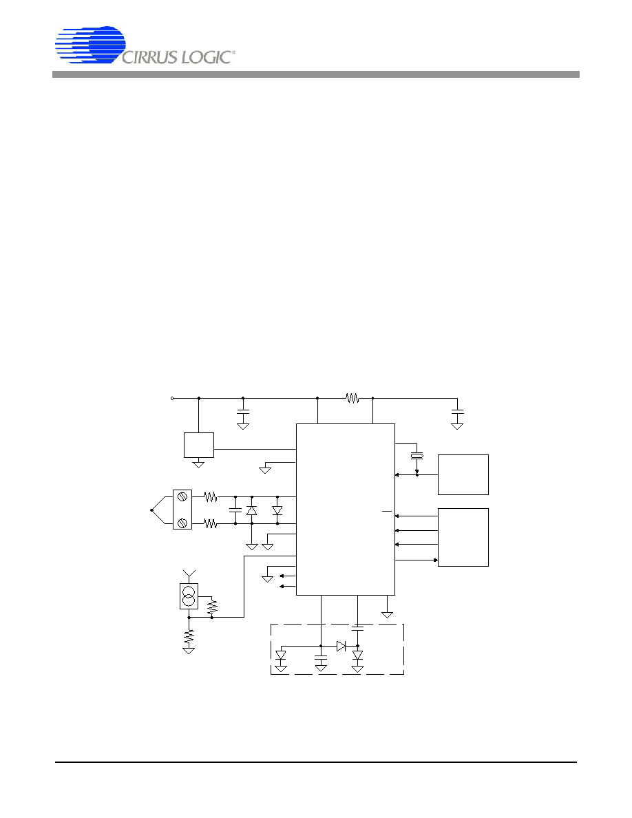
Figure 21 illustrates the CS5522 connected with a
+5 V analog supply and with the external compo-
nents required for the charge pump drive. This en-
ables the CS5522 to measure ground-referenced
signals with magnitudes down to ±100 mV.
Figure 22 illustrates the CS5522 connected to mea-
sure ground-referenced unipolar signals of a posi-
tive polarity using the 1 V, 2.5 V, and 5 V ranges
on the converter. For the 25 mV, 55 mV, and
100 mV ranges, the signals being digitized must
have a common mode between +1.85 to +2.65 V
(NBV = 0 V).
Although CS5521/22/23/24/28 are optimized for
the measurement of thermocouple outputs, they are
also well suited for the measurement of ratiometric
bridge transducer outputs. Figure 23 illustrates the
CS5522 connected to measure the output of a rati-
ometric differential bridge transducer while operat-
ing from a single +5 V supply. Bridge outputs may
range from 5 mV to 400 mV. See “Digital Gain
Scaling” on page 45 section about manipulating the
gain register to achieve optimum gain scaling.
XO U T
VD +
VA +
VR E F +
VR E F -
DG ND
NB V
AIN 1 +
SC L K
SD O
SD I
C S 5522
XIN
CP D
CS
10
Ω
+5 V
An a lo g
Su p p ly
0.1
μF0 .1 μF
20
19
3
1
AG N D
21 4
11
10
15
12
8
9
13
5
O p tion al
Clo c k
S ourc e
Se ria l
Da ta
In te rfa ce
7
32 .7 68 ~ 1 0 0 k H z
2.5 V
U p to ± 1 00 m V In pu t
AIN 1 -
4
10 k
Ω
0.1
μF
10
μF
1 N 4148
1 N 41 48
+
BA V 1 9 9
18
AIN2 +
17
AIN 2 -
16
A1
6
A0
C harg e -p um p n e tw o rk
fo r V D + = 5 V o n ly a n d
X IN = 32.76 8 k H z .
Lo g ic O u tp u ts :
A0 - A 1 S w itc h fro m
V A + to A G ND.
10 k
Ω
301
Ω
49 9
Ω
+5 V
V+
R
LM 334
Ab s o lu te
Cu rre n t
R e fe renc e
V-
C o ld J u nction
BA T 8 5
0.0 33
μF
Figure 21. CS5522 Configured to use on-chip charge pump to supply NBV
发布紧急采购,3分钟左右您将得到回复。
相关PDF资料
CS5529-ASZR
IC ADC 16BIT W/6BIT LATCH 20SSOP
CS5530-ISZR
IC ADC 24BIT 1CH W/LNA 20-SSOP
CS5534-ASZR
IC ADC 24BIT 4CH W/LNA 24-SSOP
CS5534-BSZR
IC ADC 24BIT 4CH W/LNA 24SSOP
CS5550-ISZR
IC ADC 2CH LOW-COST 24-SSOP
CS5565-ISZ
IC ADC DELTA-SIGMA 24BIT 24-SSOP
CY28317PVXC-2
IC CLK FTG VIA PL/E133T 48SSOP
CY28323OXC
IC CLOCK BROOKDALE GPENT4 48SSOP
相关代理商/技术参数
CS5529
制造商:CIRRUS 制造商全称:Cirrus Logic 功能描述:16 BIT PROGRAMMABLE ADC WITH 6 BIT LATCH
CS5529_05
制造商:CIRRUS 制造商全称:Cirrus Logic 功能描述:16-bit, Programmable ΔΣ ADC with 6-bit Latch
CS5529-AP
功能描述:模数转换器 - ADC Prgrmmbl Delta Sigma ADC w/6-Bit Lat-Ch RoHS:否 制造商:Texas Instruments 通道数量:2 结构:Sigma-Delta 转换速率:125 SPs to 8 KSPs 分辨率:24 bit 输入类型:Differential 信噪比:107 dB 接口类型:SPI 工作电源电压:1.7 V to 3.6 V, 2.7 V to 5.25 V 最大工作温度:+ 85 C 安装风格:SMD/SMT 封装 / 箱体:VQFN-32
CS5529AS
制造商:CIRRUS 功能描述:New
CS5529-AS
功能描述:模数转换器 - ADC Prgrmmbl Delta Sigma ADC w/6-Bit Lat-Ch RoHS:否 制造商:Texas Instruments 通道数量:2 结构:Sigma-Delta 转换速率:125 SPs to 8 KSPs 分辨率:24 bit 输入类型:Differential 信噪比:107 dB 接口类型:SPI 工作电源电压:1.7 V to 3.6 V, 2.7 V to 5.25 V 最大工作温度:+ 85 C 安装风格:SMD/SMT 封装 / 箱体:VQFN-32
CS5529-ASZ
功能描述:模数转换器 - ADC Prgrmmbl Delta Sigma ADC w/6-Bit Lat-Ch RoHS:否 制造商:Texas Instruments 通道数量:2 结构:Sigma-Delta 转换速率:125 SPs to 8 KSPs 分辨率:24 bit 输入类型:Differential 信噪比:107 dB 接口类型:SPI 工作电源电压:1.7 V to 3.6 V, 2.7 V to 5.25 V 最大工作温度:+ 85 C 安装风格:SMD/SMT 封装 / 箱体:VQFN-32
CS5529-ASZR
功能描述:模数转换器 - ADC IC Prgrmbl Dlt Sigma ADC w/6-Bit Latch RoHS:否 制造商:Texas Instruments 通道数量:2 结构:Sigma-Delta 转换速率:125 SPs to 8 KSPs 分辨率:24 bit 输入类型:Differential 信噪比:107 dB 接口类型:SPI 工作电源电压:1.7 V to 3.6 V, 2.7 V to 5.25 V 最大工作温度:+ 85 C 安装风格:SMD/SMT 封装 / 箱体:VQFN-32
CS5530
制造商:Texas Instruments 功能描述: